This hardware project consists of a ready made printed circuit board (available separately) which, when populated by the following list of parts forms a 24bBC address decoding board.
Building such a board from scratch on strip board makes quite a large final board so by using surface-mounted parts, the physical six of the board can be reduced to 3" by 3.5". Anyone wishing to build one from scratch can do so by consulting the 24bBC document.
A 24 bit address bus has 16 million unique addresses, half of which have been set aside for a fast RAM disk with associated RAM filing system (available separately). So about a third of this 3" by 3.5" board is occupied by sockets for RAM chips for this purpose.
Operation of this design is covered in the 24bBC article elsewhere on this disk.
Parts
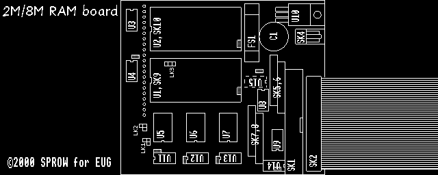
The schematic shows an outline of the following parts and their relative positions on the board:
3 x 74ALS990 in SOIC package (U5,6,7)
4 x 74HC02 in SOIC package (U11,12,13,9)
1 x 74HC139 in SOIC package (U8)
1 x 74HC00 in SOIC package (U14)
1 x 74HC138 in SOIC package (U3)
1 x 4075BE in SOIC package (U15)
1 x 470uF capacitor, radial leads (C1)
1 x 1.3mm PCB mount power socket (SK4)
8 x 100nF capacitor in 0805 outline (Grey shaded areas)
1 x 34 pin IDC header (SK2)
1 x Fuse holder plus 200mA fuse (FS1)
2 x Turned pin 32 pin DIL chip sockets (SK9,10 - can be omitted)
1 x 34 pin IDC plug
2 feet of 34 way ribbon cable
If there are known to be no other boxes on the 1MHz bus then the card must be terminated with:
4 x 9 pin SIL array 2.2k resistor packs
If there are other devices daisy chained through the board then you will need a socket for the next device to plug into:
1 x 34 pin board mount non locking IDC socket (SK1)
If there might be devices daisy chained on the 1MHz bus some of the time and sometimes not, the terminating resistors should be socketed too:
4 x 9 pin SIL array 2.2k resistor packs
1 x 34 pin board mount non locking IDC socket (SK1)
4 x Turned pin 9 way SIL socket (SK5,6,7,8)
The amount of RAM fitted is entirely optional, and automatically detected by the RAM filing system software:
1 or 2 x KM681000 (128k x 8bit SRAM) or equivalent in a 32 pin DIL package
1 or 2 x KM684000 (512k x 8bit SRAM) or equivalent in a 32 pin DIL package
Optional parts not required by the RAM disk (see below)
1 x 74HC138 (U4)
1 x 7805 voltage regulator in TO220 case (U10)
Benefits
- Tiny design is even smaller than a 3.5" floppy disk
- Very low power, drawing only 125mA
- Special 21 pin expansion header gives the designer the option to add other peripherals to the 24bBC bus or even more RAM
- Potentially up to 1 Megabyte of storage on board (or 8 Megabytes using the expansion header)
Build
Because of the orientation of the surface mounted components they must be assembled in a particular order so that there is plenty of room for the soldering iron tip when placing neighbouring devices.
- Fit U14,U9,U8,U13,U7,U12,U6,U11,U5,U3 (and U4 if required)
- Fit the surface mount decoupling capacitors, some of which are on the reverse of the board
- Fit U15 which is on the reverse of the board
- Fit SK5,SK6,SK7,SK8 if required, or the 2.2k resistor arrays if the terminators are not to be socketed
- Depending on which RAM configuration is being used, there are some option links to alter. By default the tracks are laid out for the 512k devices, so LK1,LK2,LK3 are all made in the '4' position (this is marked on the PCB next to the links). For 128k devices, break these links with a knife and put a link made from an off cut of the capacitor's leads into the '1' position
- Now fit SK9,SK10 if required
- Fit C1,FS1,SK4 to complete the placement
- If you are not running the board from a 5v supply there needs to be a regulator fitted in the place of U10. To enable the regulator you must first cut the 'U' shaped track on the rear of the board going between pins 1 and 3 of U10 which bypasses U10 when it is not required (the default)
Hints
- Soldering surface mount components is easy - it requires a steady hand and a good soldering iron tip. Don't try to solder with one shaped like a marker pen or a chisel, you need a pointed one shaped like a very slim cone. Smear a little flux or solder paste onto the pads where the device is to go and sit the chip in place so that you're happy it lines up with the pads. Hold the chip still by pressing on the top with a flat head screwdriver, and dab a little solder on the diagonally opposite corner pins (eg. pin 1 & 14). This anchors the device.
Make any minor adjustments by melting one of those two pins and nudging the chip into line, then when happy put solder on the remaining pins. Now clean the excess flux off and inspect the joints. - To crimp the 34 pin IDC header without crushing the pins put the ribbon cable through the plug and satisfy yourself it is lined up straight. Put the assembly into a vice, and put a few matchsticks between the pins. Then, when closing the vice, the pressure is applied to the matchstick which transfers it to the plastic casing without bending any pins.
- If only one of the possible two RAMs is installed, put it in the socket marked RAM0 first (not RAM1). Do not mix 128k & 512k devices.
- If you need to cut links LK1 and LK2 are on the back of the board whereas LK3 is on the top side.
As always, happy soldering!
Robert Sprowson, EUG #56