Latches
The limited expansion capabilities of an 8 bit addon on the 1MHz connector on the BBC micro are easily overcome with some latches.
A fully decoded 24 bit address bus is presented here, giving up to 16 million unique locations! Half of this (8Mb) has been allocated as RAM for a fast RAM disk.
It's up to the user's imagination to decide what input/output devices are connected to the other 8 million locations - some suggestions are a real time clock, your favourite ROM images, extra serial/parallel ports, a TV card, etc...
Parts
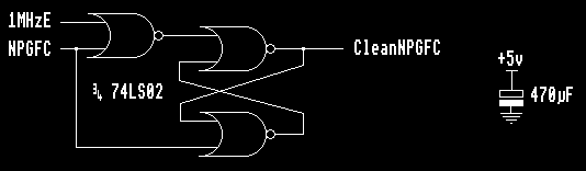
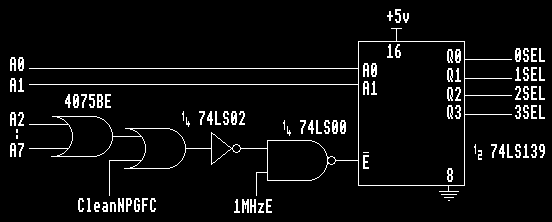
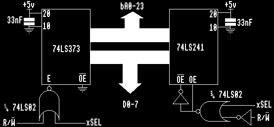
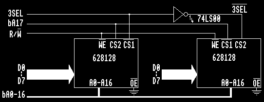
The slideshow of circuit diagrams in the Utilities Menu show how to assemble the unit electrically. It requires the following parts:
| 3 | x | 74LS373 latches |
| 3 | x | 74LS241 tristate buffers |
| 4 | x | 74LS02 |
| 1 | x | 74LS00 |
| 1 | x | 4075BE |
| 1 | x | 470uF capacitor |
| 6 | x | 33nF capacitors |
| 1 | x | 34 way IDC connector,and ribbon cable |
| 2 | x | 3.3k resistor packs (8 resistors to a pack) |
| 1 | x | stripboard, solder and wires |
In addition, the prototype RAM disk used 2 x 628128 SRAM chips (i.e. 256k in total), though any combination up to 8Mb can be added with a little extra circuitry.
Benefits
- Single board decodes and cleans up all the 1MHz bus signals making future projects easier to build
- Can be mounted internally to the case
- Use of a diode and 4.5v battery makes the RAM disk permanent
- No more grinding of precious floppy disks
- Fully featured RAM filing system already available
How To Build
- Carefully consult the circuit diagram and manufacturers' data sheets displayed at the bottom of this article for the logic ICs, to arrive at a strip board layout.
- Be sure to terminate the data bus with 3.3k resistors to 5v and 0v to stop reflections over long cable lengths.
- The decoupling capacitors (33nF) should be mounted as close to the latch and tristate buffers as possible to stop noise on the power lines.
- It's arbitary which latches and tristate buffers you use for each of the eight data lines from the BBC,but be consistent and label the final board!
- The RAM chips are best mounted on a small 'daughter' board as this makes the wiring from the latches to the RAM address lines easier - busses are very hard to implement on stripboard.
- It's arbitary which order the RAM address lines are joined to the main board since bytes will be read back from the same place they were written, so it doesn't matter.
- The board should be attached to a regulated supply capable of supplying about 250mA.
Hints
- Below around 2.5v the contents of SRAM may become corrupted or lost.
- You can dramatically reduce the number of chips you need and (more so) the wiring between the chips by use of 74ALS990 read/write buffers.
- The board appears at &FC00, &FC01, &FC02 for the three address registers which is the 'test hardware' allocation in the 1MHz bus memory map. Read/writes to the RAM occur at &FC03.
- The use of both latches and read back tristate buffers makes ?&FC00=?&FC00+1 in BASIC possible, or INC&FC00 in assembler which have great speed increases over having to keep copies of the registers in the BBC's RAM
- Interrupt routines concerned with hardware on the 24bBC board must preserve the current address by reading FC00/01/02,and restoring this before exiting.
Figures
Happy soldering!
Robert Sprowson
If you're not confident enough to build this piece of hardware yourself, Robert Sprowson is offering a ready-made board service. Read his letter for more details.Dave E, EUG #50